1. 课程信息
实验地点:清水河校区KB239
**实验时间:**2021.04.9
实验时长: 3小时(4节课)
2. 实验要求
驱动板上数码管显示当前时间(包含时、分、秒)
①建议定义n个按键,如用于功能切换 (tab)、校时+1(up)及确认(ok)
②整点报时: 7:00~23:00间每个整点蜂鸣器响1s
思考(加分项):
1. 如何添加闹钟功能?
2. 如何添加定时器功能?
3. 设计模N计数器的测试向量集,撰写testbench进行验证测试
3. 设计与实现
3.1 电路功能说明
(包括各个模块功能、关键代码分析,可以使用文字、框图、功能表、状态图等进行说明)
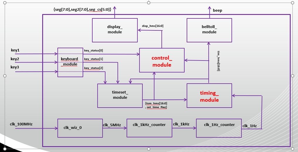
3.1.1 顶层设计
3.1.2 timing_module
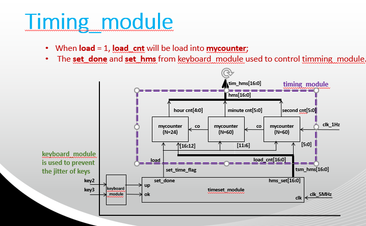
接收PLL多次分频得到的1Hz时钟信号作为模块的时钟信号,设置17位数据用来存储当前时间([5:0]表示秒,[11:6]表示分,[16:12]表示小时),当秒达到59时,则下一次操作为秒位置0,同时分位加1,分钟与小时的关系依次类推。同时当load信号使能时,即设置时间功能打开时,数据位数据将被加载进来的数据覆盖。
// timing_module.v
`timescale 1ns / 1ps
//////////////////////////////////////////////////////////////////////////////////
// Company: UESTC
// Engineer: Qy_Ley
//
// Create Date: 2021/03/14 15:06:37
// Design Name: Digital Clock for EES331
// Module Name: timing_module
// Project Name: Digital Clock
// Target Devices: EES331
// Tool Versions: Vivado 18.3
// Description:
//
// Dependencies:
//
// Revision:
// Revision 0.01 - File Created
// Additional Comments:
//
//////////////////////////////////////////////////////////////////////////////////
module timing_module(
    input i_clk_1Hz,
    input i_load,
    input i_rstn,
    input i_ena,
    input [16:0] i_load_hms,  // [5:0] for sec, [11:6] for min, [16:12] for hour, BCD coding
    output [16:0] o_hms  // [5:0] for sec, [11:6] for min, [16:12] for hour, BCD coding
);
//    wire m_co_sec, m_co_min; // Carry output from second & minute counter
    reg ld;
    reg [16:0] ld_cnt;
    reg [4:0] hour_cnt;
    reg [5:0] min_cnt,sec_cnt;
    always @(posedge i_clk_1Hz) begin
        ld <= i_load;
        ld_cnt <= i_load_hms;
    end //clock cross-domain buffer
  always @(posedge i_clk_1Hz or negedge i_rstn) begin
     if(!i_rstn) begin
         hour_cnt <= 0;
         min_cnt <= 0;
         sec_cnt <= 0;
     end
     else if(ld) begin
         {hour_cnt, min_cnt, sec_cnt} <= ld_cnt;
     end
     else if(i_ena) begin
         if(sec_cnt == 6'd59) begin
             sec_cnt <= 0;
             if(min_cnt == 6'd59) begin
                 min_cnt <= 0;
                 if(hour_cnt == 5'd23) begin
                     hour_cnt <= 0;
                 end
                 else begin
                     hour_cnt <= hour_cnt+1;
                 end
             end
             else begin
                 min_cnt <= min_cnt+1;
             end
         end
         else begin
             sec_cnt <= sec_cnt+1;
         end
     end
    end
  /* Complete the counter for second, minute, hour */
  assign o_hms = {hour_cnt, min_cnt, sec_cnt};
endmodule
3.1.3 control_module
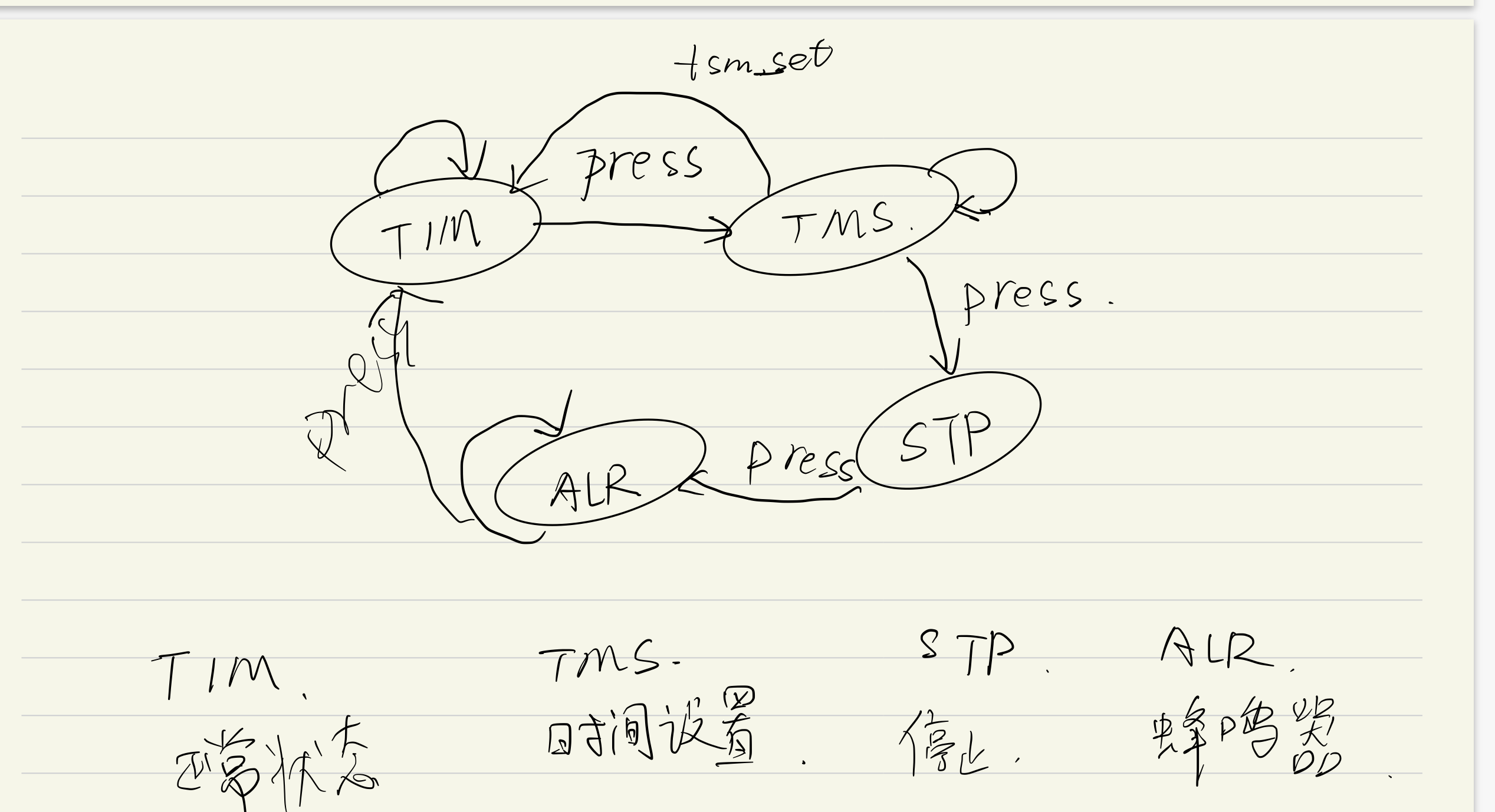
为系统控制的模块,采用有限状态机的描述方式,如图:
//  control_module.v
`timescale 1ns / 1ps
//////////////////////////////////////////////////////////////////////////////////
// Company: UESTC
// Engineer: Qy_Ley
//
// Create Date: 2021/03/14 15:06:37
// Design Name: Digital Clock for EES331
// Module Name: control_module
// Project Name: Digital Clock
// Target Devices: EES331
// Tool Versions: Vivado 18.3
// Description:
//
// Dependencies:
//
// Revision:
// Revision 0.01 - File Created
// Additional Comments:
//
//////////////////////////////////////////////////////////////////////////////////
module control_module(
    input i_clk_5MHz,
    input i_rstn,
    input i_ena,
    input i_key_tab,
    input i_tsm_set_flag, // time setting flag from Timeset module
    input [16:0] i_tim_hms, // Timing module output
    input [16:0] i_tsm_hms, // Timeset module ouput
    input [16:0] i_swm_hms, // Stopwatch module output (reserved)
    input [16:0] i_alm_hms, // Alarm module output (reserved)
    output reg [16:0] o_disp_hms, // output to display module
    output reg o_tsm_ena, // Timeset module enable
    output reg o_alm_ena
);
    reg i_key_tab_d1;
    wire tab_press;
    reg i_tsm_set_flag_d1;
    wire i_tsm_set_done;
    always @(posedge i_clk_5MHz) begin
        i_key_tab_d1 <= i_key_tab;
        i_tsm_set_flag_d1 <= i_tsm_set_flag;
    end
    assign tab_press = ^{i_key_tab_d1,i_key_tab}; // edge detect, =1 stand for tab key has been press down once
    assign i_tsm_set_done = ({i_tsm_set_flag_d1,i_tsm_set_flag}==2'b10); // negtive edge detect , =1 stand for time set finish
    // FSM Controller
    parameter TIM=2'd0, TMS=2'd1, STP=2'd2, ALR=2'd3; // i.e. TIMing, TiMe Setting, SToP watch, ALaRm  (4 funtion)
    reg [1:0] state, next_state;
    // Complete the State Tranfer Logic
    always @(*) begin
        case(state)
            TIM: begin
              //Example
                if(tab_press) next_state = TMS;
                else next_state = TIM;
            end
            TMS: begin
              //your code here
              if(tab_press) next_state = STP;
              else if(i_tsm_set_done) next_state = TIM;
                else next_state = TMS;
            end
            STP: begin
                //your code here
                if(tab_press) next_state = ALR;
                else next_state = STP;
            end
            ALR: begin
                //your code here
                if(tab_press) next_state = TIM;
                else next_state = ALR;
            end
        endcase
    end
    // State Transfer Block
    always @(posedge i_clk_5MHz) begin
        if(~i_rstn) state <= TIM;
        else state <= next_state;
    end
    //Complete the Output of each State
    always @(posedge i_clk_5MHz) begin
        case(next_state)
            TIM: begin
              //your code here
              o_tsm_ena <= 0;
              o_alm_ena <= 0;
                o_disp_hms <= i_tim_hms;
          end
            TMS: begin
              //your code here
              o_tsm_ena <= 1;
              o_alm_ena <= 0;
                o_disp_hms <= i_tsm_hms;
            end
            STP: begin
              //your code here
              o_tsm_ena <= 0;
              o_alm_ena <= 0;
                o_disp_hms <= i_swm_hms;
            end
            ALR: begin
              //Example
              o_tsm_ena <= 0;
              o_alm_ena <= 1;
              o_disp_hms <= i_alm_hms;
            end
        endcase
    end
endmodule
3.2 电路接口定义
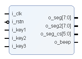
顶层的接口信号定义如下表 1所示。
表 1 顶层接口定义
| 信号名称 | 信号位宽(bit) | 信号方向(I/O) | 信号功能描述 |
|---|---|---|---|
| i_clk | 1 | I | 100MHz系统时钟 |
| i_rstn | 1 | I | 复位信号 |
| i_key1, i_key2, i_key3 | 1 | I | 3个按键输入 |
| o_seg, o_seg2 | 8 | O | 两个段选信号 |
| o_seg_cs | 6 | O | 位选信号 |
| o_beep | 1 | O | LED使能,代替蜂鸣器的输出 |
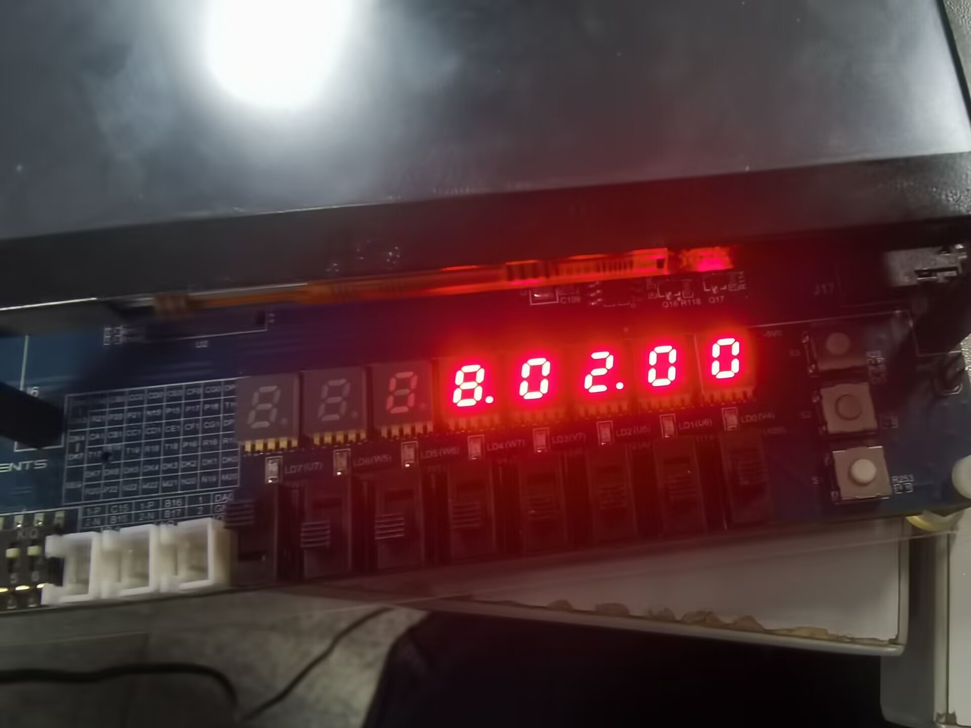
4. 实验结果
(可以使用综合后RTL图等实验过程截屏,实物照片等)
5. 实验中遇到的问题及解决方法
又又又一次一个变量在多个always块中赋值导致下板失败。解决办法为将多个always块合并为一个。
6. 实验感想和建议
数字钟的设计更多关注于顶层设计,比起流水灯的实验,模块更多且更为复杂,同时通过调用IP核来实现分频,但为了在有限的时间内完成实验内容,多个模块都没有关注内部的实现逻辑,例如数码管的段选,位选模块。而将精力集中在timing_module和control_module中。
The end